As the calendar turns to 2026, the artificial intelligence industry is witnessing a tectonic shift in its hardware foundation. The era of treating memory as a standardized commodity has officially ended, replaced by a high-stakes "HBM Scramble" that is reshaping the global semiconductor landscape. Leading the charge, Samsung Electronics (KRX: 005930) and SK Hynix (KRX: 000660) have finalized their 2026 DRAM strategies, pivoting aggressively toward customized High-Bandwidth Memory (HBM4) to satisfy the insatiable appetites of cloud giants like Google (NASDAQ: GOOGL) and Microsoft (NASDAQ: MSFT). This alignment marks a critical juncture where the memory stack is no longer just a storage component, but a sophisticated logic-integrated asset essential for the next generation of AI accelerators.
The immediate significance of this development cannot be overstated. With mass production of HBM4 slated to begin in February 2026, the transition from HBM3E to HBM4 represents the most significant architectural overhaul in the history of memory technology. For hyperscalers like Microsoft and Google, securing a stable supply of this bespoke silicon is the difference between leading the AI frontier and being sidelined by hardware bottlenecks. As Google prepares its TPU v8 and Microsoft readies its "Braga" Maia 200 chip, the "alignment" of Samsung and SK Hynix’s roadmaps ensures that the infrastructure for trillion-parameter models is not just faster, but fundamentally more efficient.
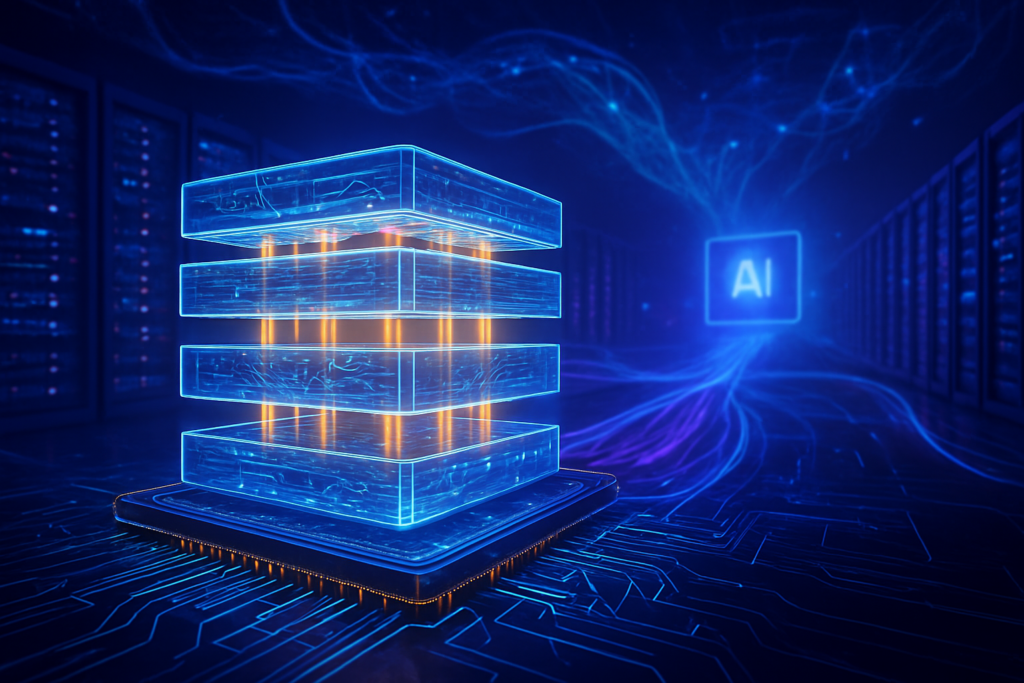
The Technical Leap: HBM4 and the Logic Die Revolution
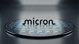
The technical specifications of HBM4, finalized by JEDEC in mid-2025 and now entering volume production, are staggering. For the first time, the "Base Die" at the bottom of the memory stack is being manufactured using high-performance logic processes—specifically Samsung’s 4nm or TSMC (NYSE: TSM)’s 3nm/5nm nodes. This architectural shift allows for a 2048-bit interface width, doubling the data path from HBM3E. In early 2026, Samsung and Micron (NASDAQ: MU) have already reported pin speeds reaching up to 11.7 Gbps, pushing the total bandwidth per stack toward a record-breaking 2.8 TB/s. This allows AI accelerators to feed data to processing cores at speeds previously thought impossible, drastically reducing latency during the inference of massive large language models.
Beyond raw speed, the 2026 HBM4 standard introduces "Hybrid Bonding" technology to manage the physical constraints of 12-high and 16-high stacks. By using copper-to-copper connections instead of traditional solder bumps, manufacturers have managed to fit more memory layers within the same 775 µm package thickness. This breakthrough is critical for thermal management; early reports from the AI research community suggest that HBM4 offers a 40% improvement in power efficiency compared to its predecessor. Industry experts have reacted with a mix of awe and relief, noting that this generation finally addresses the "memory wall" that threatened to stall the progress of generative AI.
The Strategic Battlefield: Turnkey vs. Ecosystem
The competition between the "Big Three" has evolved into a clash of business models. Samsung has staged a dramatic "redemption arc" in early 2026, positioning itself as the only player capable of a "turnkey" solution. By leveraging its internal foundry and advanced packaging divisions, Samsung designs and manufactures the entire HBM4 stack—including the logic die—in-house. This vertical integration has won over Google, which has reportedly doubled its HBM orders from Samsung for the TPU v8. Samsung’s co-CEO Jun Young-hyun recently declared that "Samsung is back," a sentiment echoed by investors as the company’s stock surged following successful quality certifications for NVIDIA (NASDAQ: NVDA)'s upcoming Rubin architecture.
Conversely, SK Hynix maintains its market leadership (estimated at 53-60% share) through its "One-Team" alliance with TSMC. By outsourcing the logic die to TSMC, SK Hynix ensures its HBM4 is perfectly synchronized with the manufacturing processes used for NVIDIA's GPUs and Microsoft’s custom ASICs. This ecosystem-centric approach has allowed SK Hynix to secure 100% of its 2026 capacity through advance "Take-or-Pay" contracts. Meanwhile, Micron has solidified its role as a vital third pillar, capturing nearly 20% of the market by focusing on the highest power-to-performance ratios, making its chips a favorite for energy-conscious data centers operated by Meta and Amazon.
A Broader Shift: Memory as a Strategic Asset
The 2026 HBM scramble signifies a broader trend: the "ASIC-ification" of the data center. Demand for HBM in custom AI chips (ASICs) is projected to grow by 82% this year, now accounting for a third of the total HBM market. This shift away from general-purpose hardware toward bespoke solutions like Google’s TPU and Microsoft’s Maia indicates that the largest tech companies are no longer willing to wait for off-the-shelf components. They are now deeply involved in the design phase of the memory itself, dictating specific logic features that must be embedded directly into the HBM4 base die.
This development also highlights the emergence of a "Memory Squeeze." Despite massive capital expenditures, early 2026 is seeing a shortage of high-bin HBM4 stacks. This scarcity has elevated memory from a simple component to a "strategic asset" of national importance. South Korea and the United States are increasingly viewing HBM leadership as a metric of economic competitiveness. The current landscape mirrors the early days of the GPU gold rush, where access to hardware is the primary determinant of a company’s—and a nation’s—AI capability.
The Road Ahead: HBM4E and Beyond
Looking toward the latter half of 2026 and into 2027, the focus is already shifting to HBM4E (the enhanced version of HBM4). NVIDIA has reportedly pulled forward its demand for 16-high HBM4E stacks to late 2026, forcing a frantic R&D sprint among Samsung, SK Hynix, and Micron. These 16-layer stacks will push per-stack capacity to 64GB, allowing for even larger models to reside entirely within high-speed memory. The industry is also watching the development of the Yongin semiconductor cluster in South Korea, which is expected to become the world’s largest HBM production hub by 2027.
However, challenges remain. The transition to Hybrid Bonding is technically fraught, and yield rates for 16-high stacks are currently the industry's biggest "black box." Experts predict that the next eighteen months will be defined by a "yield war," where the company that can most reliably manufacture these complex 3D structures will capture the lion's share of the high-margin market. Furthermore, the integration of logic and memory opens the door for "Processing-in-Memory" (PIM), where basic AI calculations are performed within the HBM stack itself—a development that could fundamentally alter AI chip architectures by 2028.
Conclusion: A New Era of AI Infrastructure
The 2026 HBM scramble marks a definitive chapter in AI history. By aligning their strategies with the specific needs of Google and Microsoft, Samsung and SK Hynix have ensured that the hardware bottleneck of the mid-2020s is being systematically dismantled. The key takeaways are clear: memory is now a custom logic product, vertical integration is a massive competitive advantage, and the demand for AI infrastructure shows no signs of plateauing.
As we move through the first quarter of 2026, the industry will be watching for the first volume shipments of HBM4 and the initial performance benchmarks of the NVIDIA Rubin and Google TPU v8 platforms. This development's significance lies not just in the speed of the chips, but in the collaborative evolution of the silicon itself. The "HBM War" is no longer just about who can build the biggest factory, but who can most effectively merge memory and logic to power the next leap in artificial intelligence.
This content is intended for informational purposes only and represents analysis of current AI developments.
TokenRing AI delivers enterprise-grade solutions for multi-agent AI workflow orchestration, AI-powered development tools, and seamless remote collaboration platforms.
For more information, visit https://www.tokenring.ai/.