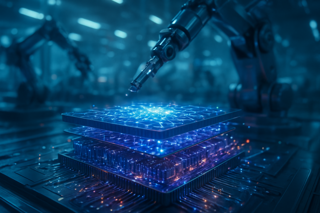
As of January 2, 2026, the global semiconductor landscape has reached a definitive turning point. After two years of "packaging-bound" constraints that throttled the supply of high-end artificial intelligence processors, Taiwan Semiconductor Manufacturing Company (NYSE: TSM) has officially entered a new era of hyper-scale production. By aggressively expanding its Chip on Wafer on Substrate (CoWoS) capacity, TSMC is finally clearing the bottlenecks that once forced lead times for AI servers to stretch beyond 50 weeks, signaling a massive shift in how the industry builds the engines of the generative AI revolution.
This expansion is not merely an incremental upgrade; it is a structural transformation of the silicon supply chain. By the end of 2025, TSMC successfully nearly doubled its CoWoS output to 75,000 wafers per month, and current projections for 2026 suggest the company will hit a staggering 130,000 wafers per month by year-end. This surge in capacity is specifically designed to meet the insatiable appetite for NVIDIA’s Blackwell and upcoming Rubin architectures, as well as AMD’s MI350 series, ensuring that the next generation of Large Language Models (LLMs) and autonomous systems are no longer held back by the physical limits of chip assembly.
The Technical Evolution of Advanced Packaging
The technical evolution of advanced packaging has become the new frontline of Moore’s Law. While traditional chip scaling—making transistors smaller—has slowed, TSMC’s CoWoS technology allows multiple "chiplets" to be interconnected on a single interposer, effectively creating a "superchip" that behaves like a single, massive processor. The current industry standard has shifted from the mature CoWoS-S (Standard) to the more complex CoWoS-L (Local Silicon Interconnect). CoWoS-L utilizes an RDL interposer with embedded silicon bridges, allowing for modular designs that can exceed the traditional "reticle limit" of a single silicon wafer.
This shift is critical for the latest hardware. NVIDIA (NASDAQ: NVDA) is utilizing CoWoS-L for its Blackwell (B200) GPUs to connect two high-performance logic dies with eight stacks of High Bandwidth Memory (HBM3e). Looking ahead to the Rubin (R100) architecture, which is entering trial production in early 2026, the requirements become even more extreme. Rubin will adopt a 3nm process and a massive 4x reticle size interposer, integrating up to 12 stacks of next-generation HBM4. Without the capacity expansion at TSMC’s new facilities, such as the massive AP8 plant in Tainan, these chips would be nearly impossible to manufacture at scale.
Industry experts note that this transition represents a departure from the "monolithic" chip era. By using CoWoS, manufacturers can mix and match different components—such as specialized AI accelerators, I/O dies, and memory—onto a single package. This approach significantly improves yield rates, as it is easier to manufacture several small, perfect dies than one giant, flawless one. The AI research community has lauded this development, as it directly enables the multi-terabyte-per-second memory bandwidth required for the trillion-parameter models currently under development.
Competitive Implications for the AI Giants
The primary beneficiary of this capacity surge remains NVIDIA, which has reportedly secured over 60% of TSMC’s total 2026 CoWoS output. This strategic "lock-in" gives NVIDIA a formidable moat, allowing it to maintain its dominant market share by ensuring its customers—ranging from hyperscalers like Microsoft and Google to sovereign AI initiatives—can actually receive the hardware they order. However, the expansion also opens the door for Advanced Micro Devices (NASDAQ: AMD), which is using TSMC’s SoIC (System-on-Integrated-Chip) and CoWoS-S technologies for its MI325 and MI350X accelerators to challenge NVIDIA’s performance lead.
The competitive landscape is further complicated by the entry of Broadcom (NASDAQ: AVGO) and Marvell Technology (NASDAQ: MRVL), both of which are leveraging TSMC’s advanced packaging to build custom AI ASICs (Application-Specific Integrated Circuits) for major cloud providers. As packaging capacity becomes more available, the "premium" price of AI compute may begin to stabilize, potentially disrupting the high-margin environment that has fueled record profits for chipmakers over the last 24 months.
Meanwhile, Intel (NASDAQ: INTC) is attempting to position its Foundry Services as a viable alternative, promoting its EMIB (Embedded Multi-die Interconnect Bridge) and Foveros technologies. While Intel has made strides in securing smaller contracts, the high cost of porting designs away from TSMC’s ecosystem has kept the largest AI players loyal to the Taiwanese giant. Samsung (KRX:005930) has also struggled to gain ground; despite offering "turnkey" solutions that combine HBM production with packaging, yield issues on its advanced nodes have allowed TSMC to maintain its lead.
Broader Significance for the AI Landscape
The broader significance of this development lies in the realization that the "compute" bottleneck has been replaced by a "connectivity" bottleneck. In the early 2020s, the industry focused on how many transistors could fit on a chip. In 2026, the focus has shifted to how fast those chips can talk to each other and their memory. TSMC’s expansion of CoWoS is the physical manifestation of this shift, marking a transition into the "3D Silicon" era where the vertical and horizontal integration of chips is as important as the lithography used to print them.
This trend has profound geopolitical implications. The concentration of advanced packaging capacity in Taiwan remains a point of concern for global supply chain resilience. While TSMC is expanding its footprint in Arizona and Japan, the most cutting-edge "CoW" (Chip-on-Wafer) processes remain centered in facilities like the new Chiayi AP7 plant. This ensures that Taiwan remains the indispensable "silicon shield" of the global economy, even as Western nations push for more localized semiconductor manufacturing.
Furthermore, the environmental impact of these massive packaging facilities is coming under scrutiny. Advanced packaging requires significant amounts of ultrapure water and electricity, leading to localized tensions in regions like Chiayi. As the AI industry continues to scale, the sustainability of these manufacturing hubs will become a central theme in corporate social responsibility reports and government regulations, mirroring the debates currently surrounding the energy consumption of AI data centers.
Future Developments in Silicon Integration
Looking toward the near-term future, the next major milestone will be the widespread adoption of glass substrates. While current CoWoS technology relies on silicon or organic interposers, glass offers superior thermal stability and flatter surfaces, which are essential for the ultra-fine interconnects required for HBM4 and beyond. TSMC and its partners are already conducting pilot runs with glass substrates, with full-scale integration expected by late 2027 or 2028.
Another area of rapid development is the integration of optical interconnects directly into the package. As electrical signals struggle to travel across large substrates without significant power loss, "Silicon Photonics" will allow chips to communicate using light. This will enable the creation of "warehouse-scale" computers where thousands of GPUs function as a single, unified processor. Experts predict that the first commercial AI chips featuring integrated co-packaged optics (CPO) will begin appearing in high-end data centers within the next 18 to 24 months.
A Comprehensive Wrap-Up
In summary, TSMC’s aggressive expansion of its CoWoS capacity is the final piece of the puzzle for the current AI boom. By resolving the packaging bottlenecks that defined 2024 and 2025, the company has cleared the way for a massive influx of high-performance hardware. The move cements TSMC’s role as the foundation of the AI era and underscores the reality that advanced packaging is no longer a "back-end" process, but the primary driver of semiconductor innovation.
As we move through 2026, the industry will be watching closely to see if this surge in supply leads to a cooling of the AI market or if the demand for even larger models will continue to outpace production. For now, the "CoWoS Crunch" is effectively over, and the race to build the next generation of artificial intelligence has entered a high-octane new phase.
This content is intended for informational purposes only and represents analysis of current AI developments.
TokenRing AI delivers enterprise-grade solutions for multi-agent AI workflow orchestration, AI-powered development tools, and seamless remote collaboration platforms.
For more information, visit https://www.tokenring.ai/.


